☎ : 9986251651
Email : training@siliconchip.in
Silicon
C
hip Technologies
FAQ's
Contact Us
Placement
Training
Course
DFT
Physical Design
Analog Layout
PDK Development
Embedded Systems
About Us
Home
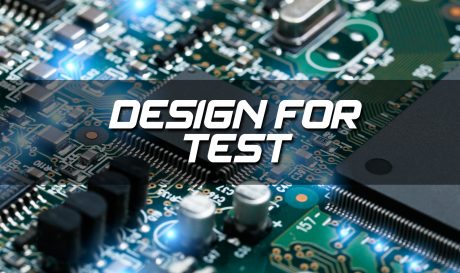
DFT (Design For Testability)
DFT Course Started...
Course Contents
WEEK-1
Full SOC flow – DFT
DFT importance in chip design
DFT Architecture and Basics
Test plan of a chip
Different DFT schemes
Comparison between Functional and DFT vectors
Week-2
DIGITAL LOGIC basics
Combination logic circuit
Sequential Logic circuit
Understand clocks and resets
Latches and D Flops functionality
Latches Waveforms
Setup time and hold time
Meta stability
PLL requirement, its operations and uses
Counters/dividers with its waveforms
Digital basic explanation
Week-3
Understanding of SCAN insertion
Scan methodology
Types of Scan
Top-down and Bottom-up Approach
Scan insertion Flow
Scan operation
Week-4
Scan insertion Scripts
Multiple Clock domains
Design Rule Checking
Pre-DRC and Post-DRC
Lockup and Terminal Lockup latches
Gated Clocks
Hands-on Scan insertion
Week-5
Introduction to Compression
Compression Architecture
Decompressor and compactor
Compression Ratio
DRC Analysis
Week-6
Modular Compression
X-Masking Logic
Hands-on Compression
Assignments
Week-7
Scan insertion with Compression
On-chip clocking for at-speed testing
Hierarchical Scan Design
Bypass mode
Hands-on scan and compression
Interaction session scan and compression
Week-8
Types of memories
Introduction to MBIST
Memory grouping
Controller generation
Memory faults
Algorithm
Diagnostic mode
Week-9
ATPG Overview
Different types of Faults
Types of fault models
ATPG Algorithm
Understand complete Test procedure
Hands-on Project
Week-10
DRC analysis
Test Coverage and Fault coverage
Coverage improvement Analysis
Chain and Capture patterns
Simulations Notiming and timing simulations
Week-11
At-speed fault model(in details)
Understanding Transition fault ATPG
Two pulse generator
Test Procedure
Launch on capture (LOC) and Launch on shift (LOS)
Top-off pattern generation
Path delay
Week-12
Introduction to JTAG
BSDL files
Difference between JTAG IEEE 1149.1 & 1149.6
JTAG state machine
GPIO & LVDS
Boundary Scan
Different instructions
Industry Standard Project
Week-13
Introduction to LBIST
Difference between Functional verification and Formal verification
Revision
Mock Interview with Industry standard questions
Mock Interview by Industry veteran 2-3 different people